
搜索结果: 1-10 共查到“半导体材料 Materials”相关记录10条 . 查询时间(0.094 秒)
复旦大学材料科学系方晓生课题组在Nature Reviews Materials期刊发表低维宽禁带半导体用于紫外光探测器的研究综述(图)
方晓生 低维宽禁带 半导体 紫外光探测器
2023/11/21
精确的紫外光检测是现代光电技术的重要组成部分,现阶段的紫外光探测器主要基于宽禁带半导体,例如,III-V半导体。然而,传统的宽禁带半导体在实际应用中达到了瓶颈,难以兼顾高集成度和高柔性。有鉴于此,低维宽禁带半导体由于具有合适的紫外光吸收范围、可调节的光电性能以及良好的衬底兼容性等优势,在多种紫外光工作场景中展现出巨大的应用潜力。
Engineers report a major advance in creating a new family of semiconductor materials(图)
半导体材料 硫族化 物钙钛矿 太阳能电池
2023/6/7
MIT engineers report creating the first high-quality thin films of a new family of semiconductor materials. The feat, which lead researcher Rafael Jaramillo refers to as his “white whale” because of h...
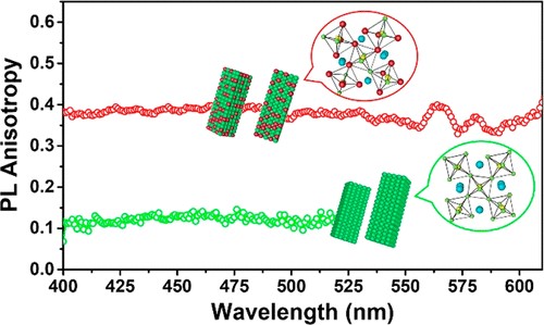
上海大学机电工程与自动化学院杨绪勇教授团队在ACS旗舰材料期刊《ACS Materials Letters》上发表研究论文(图)
上海大学机电工程与自动化学院 杨绪勇 ACS ACS Materials Letters 材料期刊
2020/7/15
近日,上海大学机电工程与自动化学院新型显示技术及应用集成教育部重点实验室杨绪勇教授课题组与香港城市大学Andrey L. Rogach教授合作在国际著名期刊《ACS Materials Letters》上在线发表论文“Lattice Distortion in Mixed-Anion Lead Halide Perovskite Nanorods Leads to their High Fluor...

中国药科大学理学院钟文英、徐波团队在Journal of Materials Chemistry A发表喹唑啉基二维有机骨架结构材料最新研究成果(图)
中国药科大学理学院 钟文英 徐波 Journal of Materials Chemistry A 喹唑啉基二维有机骨架结构材料 光伏发电 半导体
2020/4/10
近日,中国药科大学理学院钟文英教授和徐波副教授团队有关喹唑啉基二维有机骨架结构材料的最新研究成果――A two-dimensional quinazoline based covalent organic framework with a suitable direct gap and superior optical absorption for photovoltaic application...

New ultrathin semiconductor materials exceed some of silicon’s ‘secret’ powers,Stanford engineers find(图)
New ultrathin semiconductor materials silicon secret powers Stanford engineers
2017/9/5
The next generation of feature-filled and energy-efficient electronics will require computer chips just a few atoms thick. For all its positive attributes, trusty silicon can’t take us to these ultrat...
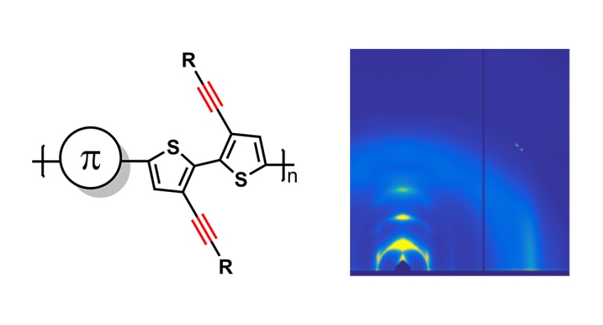
南方科技大学材料科学与工程系本科生在材料化学(Chemistry of Materials)上发表研究论文(图)
南方科技大学材料科学与工程系 材料化学 Chemistry of Materials 研究论文
2017/5/5
近日,我系郭旭岗课题组2013级本科生王雨伦同学以第一作者身份在国际材料领域一流期刊材料化学《Chemistry of Materials》(影响因子: 9.407) 上发表了关于基于头碰头链接双噻吩聚合物半导体的研究成果,论文题目为“Alkynyl-Functionalized Head-to-Head Linkage Containing Bithiophene as a Weak Donor...
Finding new functional materials is always tricky. But searching for very specific properties among a relatively small family of known materials is even more difficult.But a team from Northwestern Eng...

Stacking Two-Dimensional Materials May Lower Cost of Semiconductor Devices(图)
Two-Dimensional Materials Lower Cost Semiconductor Devices
2014/12/30
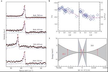
Semiconductor heterostructures provide a powerful platform to engineer the dynamics of excitons for fundamental and applied interests. However, the functionality of conventional semiconductor heterost...
石墨烯是由单层碳原子紧密堆积成二维蜂窝状晶格结构的一种碳质新材料。由于其独特的二维结构和优异的晶体学质量,石墨烯蕴含了丰富而新奇的物理现象,使其迅速成为凝聚态物理领域近年来的研究热点之一。
Center for Solar and Electronic Materials, Colorado School of Mines(图)
Center for Solar and Electronic Materials Colorado School of Mines 半导体材料 电子材料 聚合体
2007/12/24
The Center for Solar and Electronic Materials is to act as the focal point for research and education in solar and electronic materials and technology. In fulfilling its mission the center facilitates...